Krasnoyarsk scientists have learned to grow nanocrystals with a given shape
9 June 2020 г.

Iron and silicon belong to the most abundant elements in the earth's crust; therefore, nanostructures based on these materials are most accessible. They are environmentally friendly elements and have a wide range of possible applications in various fields of electronics and photonics. However, for their effective use, it is necessary to create nanocrystals with controlled variable properties.
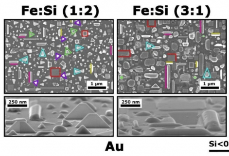
Scientists at the Federal Research Center KSC SB RAS developed a new method for growing iron silicide nanocrystals, which allows one to obtain rectangular and triangular structures with size from 30 to 1500 nanometers. The method consists in the deposition of a gold coating on silicon substrates. Deposition of iron and silicon in various proportions on the surface obtained allows one to obtain crystals of a given shape.
A thin layer of gold preliminarily deposited on the silicon surface makes it possible to control the shape and orientation of growing nanocrystals. Gold atoms, capturing the surrounding chemical elements, become centers of the crystal formation. In this case, the precious metal particles transform the interactions of molecules on the faces of the nanocrystal, thereby changing the principle of its growth. The number of attached atoms decreases from the surface of the substrate to the apex, and on the contrary, increases on the side faces. As a result, the object does not increase in height, but forms new faces. Due to this effect, crystals appear in the form of rectangular and triangular nanoplates on the substrate. The researchers note that nanostructures of similar forms are synthesized only on a surface with gold deposited on it.
“The objects we obtained can be used in various nanoelectronic devices. Nanocrystals of iron silicide with different facets allow one to bind other materials with silicon, which is the main material for electronics. They can be used as electrical nanoscale contacts in semiconductors with low, unintended current resistance. Also, such materials can be used to create nanowires or to grow infrared light-emitting diodes. Due to their environmental safety, metal silicide crystals with a variable shape and orientation will be useful for developing laser diodes in fiber optic links. Another important result is that they can be used for the subsequent synthesis of other nanoparticles and materials, ”says Ivan Tarasov, Candidate of Physical and Mathematical Sciences, researcher at the L.V. Kirensky Institute of Physics KSC SB RAS.
The study was supported by the Russian Science Foundation, Russian Foundation for Basic Research and Government of the Krasnoyarsk Region.
Share:
